Device testing
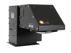
Class AAA solar simulator
The Newport 94043A is the Sol3A Class AAA Solar Simulator with a 450 Watt Xenon, Ozone Free source illuminated over a 4 inch x 4 inch area. The system is integrated to glovebox used for testing solar cell devices, has LabVIEW written software for testing J-V measurements, and flexibility for testing more than one device simultaneously.
Examples of use:
Solar cell measurements.
Purpose:
Testing solar cell devices.
Material systems:
Flexibility for testing more than one device simultaneously.
Scale/volume:
4 inch x 4 inch (101.6 mm x 101.6 mm) light illumination area.
Specifications/resolution:
Xenon Arc lamp: 450 W
Output power: 100 mW/cm2 (1.0 Sun) with variable attenuator down to 0.1 Sun
AM1.5G air mass filter
Certified to IEC 60904-9 Edition 2 (2007), JIS 8904-9 (2017), and ASTM E927-10 (2015) standards for Spectral Match, Spatial Non-Uniformity of Irradiance, and Temporal Instability of Irradiance.
Model:
Site:
The University of Queensland
Location:
Room 913, Level 9, COPE (Bldg #68), St Lucia
Instrument Contact:
Four point probe
The Keithlink four point probe is composed of a table top 4 point prober with a 4 point probe head for manual probing. The software can base on the sample geometry and thickness to measure out Resistance [W], Sheet Resistance [W/□], Volume Resistivity [W-cm], and Conductivity [S-cm-1].
Examples of use:
Film resistance measurement.
Purpose:
Electrical device characterisation
Material systems:
Electronic devices and materials.
Scale/volume:
Single chip or wafer.
Specifications/resolution:
1 mm spacing tungsten carbide probes (150 µm radius).
Model:
Site:
The University of Queensland
Location:
Room 908, Level 9, COPE (Bldg #68), St Lucia
Instrument Contact:
 Semiautomatic probe station
The Semiprobe SA-6 is a high speed tabletop probing system designed to provide reliable accurate wafer probes for 6” wafers or smaller. Ideally suited for tabletop production applications, the SA-6 is configurable for RF/microwave, failure analysis, MEMS, optoelectronics, discrete device characterisation, and R & D applications. The probe station is integrated with our device testing glove box.
Examples of use:
- Failure analysis
- Device characterisation
Purpose:
Fast semiautomatic probing station for testing and characterisation of circuitry devices and displays.
Material systems:
Electronic devices and materials.
Scale/volume:
Single 6” wafer or smaller.
Specifications/resolution:
4 probe DC probe station for measuring electrical properties of materials and devices.
Model:
Site:
The University of Queensland
Location:
Room 910, Level 9, COPE (Bldg #68), St Lucia
Instrument Contact:
 Semiconductor device analyser
The Agilent B1500A Semiconductor Device Analyser is an all in one analyser supporting IV, CV, pulse/dynamic IV and more, which is designed for all-round characterisation from basic to cutting-edge applications. It provides a wide range of measurement capabilities to cover the electrical characterisation and evaluation of devices, materials, semiconductors, active/passive components, or virtually any other type of electronic device with uncompromised measurement reliability and efficiency.
The easyexpert software provides a wide array of measurement functions: sweep/spot, multichannel sweep, list sweep, time sampling, quasi-static CV, high frequency CV (to 5 MHz), and a direct control mode. Easyexpert is also supplied with an extensive library of over 230 application tests.
Examples of use:
Characterisation of transistors, diodes, photonic devices, etc.
Purpose:
A device analyser for testing of organic and electronic circuits.
Scale/volume:
Single sample.
Specifications/resolution:
Testing of electronic devices down to 10 FA.
Model:
Site:
The University of Queensland
Location:
Room 110, Level 1, Parnell (Bldg #7), St Lucia
Instrument Contact:
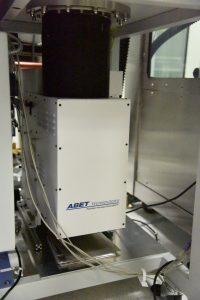
 Solar cell QE/IPCE/IV measurement system
The PV Measurements QEX7 Quantum Efficiency(QE)/Spectral Response(SR)/Incident Photon to Current Conversion Efficiency(IPCE)/IV Measurement System is a low-cost, high-performance quantum efficiency measurement system, which is capable of delivering high speed measurements on most types of solar cells. The system is designed for fast, high accuracy measurements of dye sensitized, Perovskite, crystalline and amorphous silicon, CdTe, and similar devices. The system is integrated with our device testing glove box.
The QEX7 uses a xenon arc lamp source, monochromator, filters and reflective optics to provide stable monochromatic light to a photovoltaic test device. A broadband bias light also illuminates the test device to simulate end-use conditions. The system uses a detection circuit designed to maximize measurement speed and accuracy for solar cell development.
 IV measurement feature
The integrated current–voltage (IV) measurement enables the system to perform IV measurements on small devices, without changing any electrical connections or remounting the sample. For measurements with approximated light intensities, the built-in bias light can be used as the light source. Higher accuracy measurements can be achieved using a separate solar simulator, available from PV Measurements. Maximum current is 200 mA.
Examples of use:
Solar cell measurements.
Purpose:
Solar cell characterisation.
Material systems:
Any.
Scale/volume:
Single solar cell.
Specifications/resolution:
- 300 nm to 1 100 nm scan range (1 400 nm range available)
- High resolution scan in under 1 minute
- Probe beam from 1 mm to 20 mm
- Seamless switching between DC and AC measurement modes
- 1 Hz to 120 Hz chopping frequency
- CE marked
- One white bias light
- Integrated IV measurement
Model:
PV Measurements QEX7 QE/SR/IPCE/IV Measurement System
Site:
The University of Queensland
Location:
Room 910, Level 9, COPE (Bldg #68), St Lucia
Instrument Contact:
 Wire bonder
The TPT HB16 Wire Bonder is used with gold, aluminium, silver and copper wire and ribbon. It is particularly appropriate for high quality applications requiring tight control of wire length and loop formation.
The HB16 offers direct access and simple adjustment of all bond parameters and programmable loop formation along with the capability of using a wide variety of wires. The bonding head, with the deep access option and tail adjust system, makes it ideal for deep cavity microwave applications where tight control over the tail length is required.
Examples of use:
Microwave, chip on board.
Purpose:
Packaging and microelectronics interfacing of devices to prototype level.
Material systems:
Gold, silver, aluminium, copper.
Scale/volume:
Single sample bonding.
Specifications/resolution:
Wire sizes from 17 µm to 75 µm; ribbon sizes up to 25 x 250 µm.
Deep-access wedge 16 mm and ball 13 mm.
Model:
Site:
The University of Queensland
Location:
PC2 Laboratory, Level 2E, AIBN (Bldg #75), St Lucia


